


Products
Passivation of semiconductors
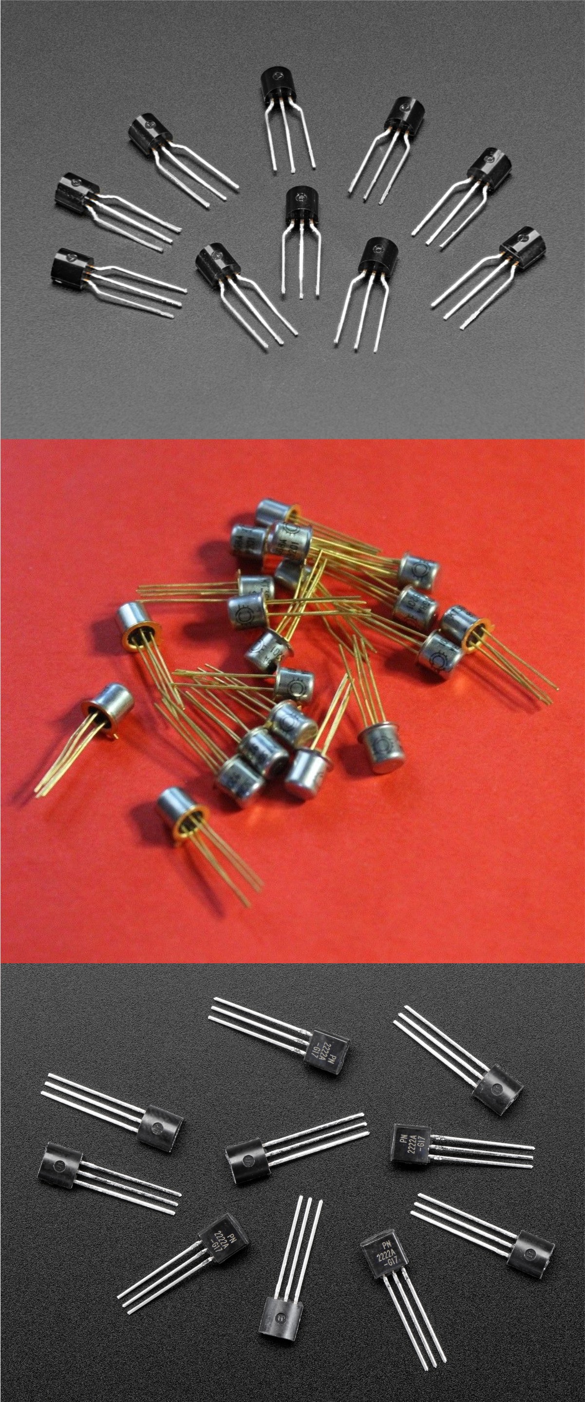
Transistor coverage increasing technical performance
Since the 80s, various research centers have been carrying out intensive work on the passivation of semiconductor devices (PP) aimed at modifying the atomic structure of the semiconductor surface
In “TESLA Crystals” LLC, based on the research carried out, a new unique (unparalleled) product has been developed: a special coverage for transistor crystals that increases the technical parameters and characteristics of transistors in many positions.
The following key points have been taken into consideration during the test:
1. Current transmission ratio (coefficient extension) at constant current
2. Maximal stresses between the collector and the ejector (in the open base)
3. Speed Frequency, up to 100000 Hz coefficient
4. Saturation voltage of emitter-collector.
All of these 4 items have been tested to include parameters that have been compared to the initial data. One of the most important results should be the increase of maximum scattering power by up to 10-15% and at the same time sufficient reduction of operating temperature limits (up to 30%) for the maximum capacity of the initial data.
Tests have shown that as a result of passivation, the operating parameters of semiconductor devices significantly increase, the leakage currents decrease by an order of magnitude and more, and, most importantly, the surface breakdown voltage rises. The latter is especially important for avalanche-forming bipolar transistors based on GaAs and other A3B5 semiconductors, since it becomes possible to completely suppress premature surface breakdown when creating high-speed electronic switches.
Passivation of the surface of test samples (25 pieces) of GaAs-based bipolar transistors was carried out by fusing at temperatures of 120-220 ° C a layer of low-melting chalcogenide glass, the thickness of which when using this method was 50 or more microns. The test results showed that passivation of the surface of transistors with low-melting chalcogenide glasses makes it possible to completely prevent surface breakdown.
The above confirms the relevance of the development of industrial technology for the formation of a passivating layer with a thickness of 1 micron and below. Such films can be obtained both by condensation from the vapor phase and by the method of deposition from solution, which is more preferable from the point of view of cheapness, simplicity and preservation of the ratio of components
In the case of successful completion of this study, the use of electronics will largely be achieved by electronic components producers, which will lead to more cost effective production.
As a positive effect, it is necessary to mention the increase of the maximum range of the electronic component parameters, the effective use of the pre-main scales, as well as the lowering of the temperature as well as the substantial increase in the quality.
Experiments were conducted on silicon and GaAs bipolar transistors as well as on diodes.
During the experiments, the experimental transistors were specially disabled. After a short time (1-2 hours), the transistors returned into their previous working state.
There are no analogues.